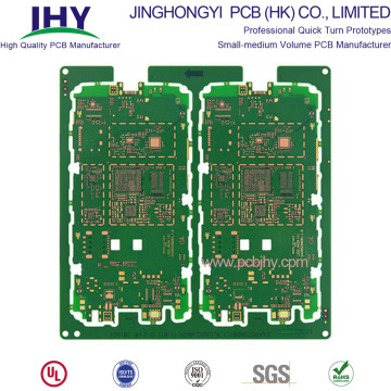
Product Name: HDI PCB Main Board of POS Machine Plate Material: FR4 Lianmao Layers: 8 Layer Plate thickness: 1.0mm Surface technology: Immersion Gold + OSP Copper thickness: 0.5oz Minimum line width / distance: 3mil/3mil Special process: Second Orders blind hole 1-2, 1-3, 6-8, 7-8 Purpose: POS Machine
HDI PCB manufacturing manufacturer
Jinghongyi PCB is a supplier and manufacturer of HDI PCB, HDI PCB prototype and multilayer HDI Rigid-Flex PCB located in Shenzhen, China, providing low-cost and high-quality HDI PCB production, manufacturing, and PCB assembly services. We have advanced HDI PCB production equipment and manufacturing process. Experienced engineers provide guidance and help for your HDI PCB design. Skilled production technicians ensure the high quality of each customized product. We have the ability to produce full-form HDI PCB for you, including: 1 + N + 1, 2 + N + 2, 3 + N + 3 and other different levels of HDI PCB. HDI PCB is a special double-layer and more than two-layer multilayer printed circuit board. With the development of miniaturization of electronic products, the application market is more and more extensive. Due to its unique process difficulty, we choose the top-grade materials(Such as RCC, LDPE, FR4), reasonable circuit layout, and the thickness can reach 1.6mm. Non-mechanical drilling, the micro-blind hole ring is below 6 mil, the wiring line width between the inner and outer layers is 4 mils, and the pad diameter is not more than 0.35 mm. Blind Via,Realize the connection and conduction between the inner layer and the outer layer. Buried Via,Realize the connection and conduction between the inner layer and the outer layer. Most of the blind holes with diameter of 0.05 and mm-0.15mm are made by laser, plasma etching and Photoforming, which are usually made by laser, and laser forming is divided into CO2 and YAG ultraviolet laser (UV). Firt order HDI PCB: After pressing once, drilling, then pressing the copper foil outside, then laser Second orders HDI PCB:After pressing once, drill holes, and then press the copper foil outside. Then laser, drill holes, and then press the copper foil outside again, and then laser. This is the second-order HDI PCB. Third orders HDI PCB:Mainly based on the number of lasers, determine the order of HDI. What is HDI PCB?
HDI (high density interconnect) is a kind of circuit board with high circuit density, which uses micro blind hole technology. HDI board has inner circuit and outer circuit, and then uses drilling, hole metallization and other processes to connect the inner circuit of each layer. HDI board is generally manufactured by the stacking method. The more the stacking times, the higher the technical grade of the board. The common HDI board is basically one-time stacking, and the high-level HDI adopts two or more times stacking technology, and at the same time, advanced PCB technologies such as stacking holes, electroplating filling holes, laser direct drilling are used. When the density of PCB increases more than eight layers, the cost of HDI is lower than that of traditional complex pressing process. HDI board is conducive to the use of advanced construction technology, and its electrical performance and signal correctness are higher than traditional PCB. In addition, HDI board has better improvement for radio frequency interference, electromagnetic wave interference, electrostatic discharge, heat conduction, etc. Electronic products continue to develop to high density and high precision. The so-called "high" not only improves the performance of the machine but also reduces the volume of the machine. High-density integration (HDI) technology can make the end product design more miniaturized and meet the higher standards of electronic performance and efficiency. At present, many popular electronic products, such as mobile phones, digital cameras, laptops, automotive electronics, etc., use HDI boards. With the upgrading of electronic products and the demand of the market, the development of the HDI board will be very rapid. The difference between HDI PCB board and ordinary PCB
PCB (printed circuit board) is an important electronic component, the support of electronic components and the carrier of electrical connection of electronic components. Because it is made by electronic printing, it is called "printed" circuit board. The common PCB board is mainly FR-4, which is made of epoxy resin and electronic glass cloth. In general, the traditional HDI needs to use adhesive-backed copper foil on the outside. Because the laser drilling cannot break through the glass cloth, the adhesive-backed copper foil without glass fiber is generally used. However, the current high-energy laser drilling machine can break through 1180 glass cloth. In this way, there is no different from ordinary materials. HDI PCB Structures
1+N+1 2+N+2 3+N+3 

How to Distinguish the First, Second and Third Orders of HDI PCB
The fabrication process of first-order HDI PCB is relatively simple and well controlled. While the second-order HDI PCB is complex due to the issue of alignment, punch and copper problem. There are a variety of second-order HDI PCB designs. One is the staggered position of the various stages which needs to connect the next-layer through the wire in the middle layer connectivity, the practice is equivalent to double first-order HDI PCB. The second is to overlap two first-order holes, thus second-order PCB is achieved by the superposition method, and the processing is also similar to the double first-order, but there are many technical points to be particularly controlled. The third is to punch directly from the outer layer to the third layer (or N-2 layer), the process is much different from the previous, and the drilling process is more difficult. For Example: The first and second order of the 6-layer board needs laser drilling, that is the HDI board. The 6-layer first-order HDI board refers to blind holes: 1-2, 2-5, 5-6. That is, 1-2, 5-6 require laser drilling. The 6-layer second-order HDI board refers to blind holes: 1-2, 2-3, 3-4, 4-5, 5-6. It requires 2 times laser drilling. First drill a buried hole of 3-4, then laminate 2-5, Then drill the 2-3, 4-5 laser holes for the first time, followed by the second laminate 1-6. Then drill the 1-2, 5-6 laser holes for the second time. Finally drill the through hole. It can be seen that the second-order HDI board has undergone two lamination and two laser drillings. Board Lamination Times: First-order PCB: one lamination is enough, just like the most common circuit board. Second-order PCB: Lamination twice. Take the example of eight-layer circuit board with blind/buried vias, laminate layer 2-7 with well-made blind/buried vias first, and then laminate layer 1 and 8 with well-made through holes. Third-order PCB: its process is much more complicated. Laminating layer 3-6 first, then layer 2 and 7, finally layer 1 and 8. It requires 3 lamination times, so most PCB manufacturers can not make it. Are PCB boards with blind holes called HDI boards?
HDI board refers to high-density interconnection circuit board. The boards of blind hole plating and secondary pressing are all HDI boards, which are divided into first-order, second-order, third-order, fourth-order and fifth-order HDI. For example, the main board of the iPhone 6 is fifth-order HDI. A simply buried hole is not necessarily HDI. Contact us if you need more details on HDI High Density PCB. We are ready to answer your questions on packaging, logistics, certification or any other aspects about HDI FR4 PCB、Immersion Gold HDI PCB. If these products fail to match your need, please contact us and we would like to provide relevant information.
Product Categories : HDI PCB